|
|
Plasmonic Photovoltaics |
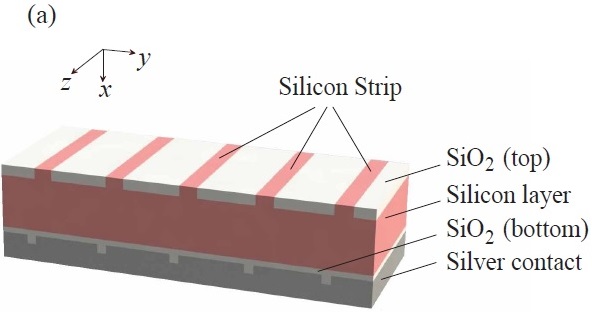
Silicon strip-loaded geometry
We show that a silicon thin-film photovoltaic structure with silicon strips on the top and grooves on the silver back contact layer can absorb incident solar energy over a broad spectral range. The silicon strips on the top scatter the incident light and significantly help couple to the photonic modes in the smaller wavelength range. The grooves on the silver back contact layer both scatter the incident light and help couple to the photonic modes and resonant surface plasmon polaritons. We find an increase of 46% in total integrated solar absorption in the proposed strip-loaded structure compared to that in a planar thin film structure of same dimensions. The proposed structure offers simpler fabrication compared to similar plasmonic-inspired designs. |
|
Extraordinary optical transmission based ultra-thin-film tandem solar cells
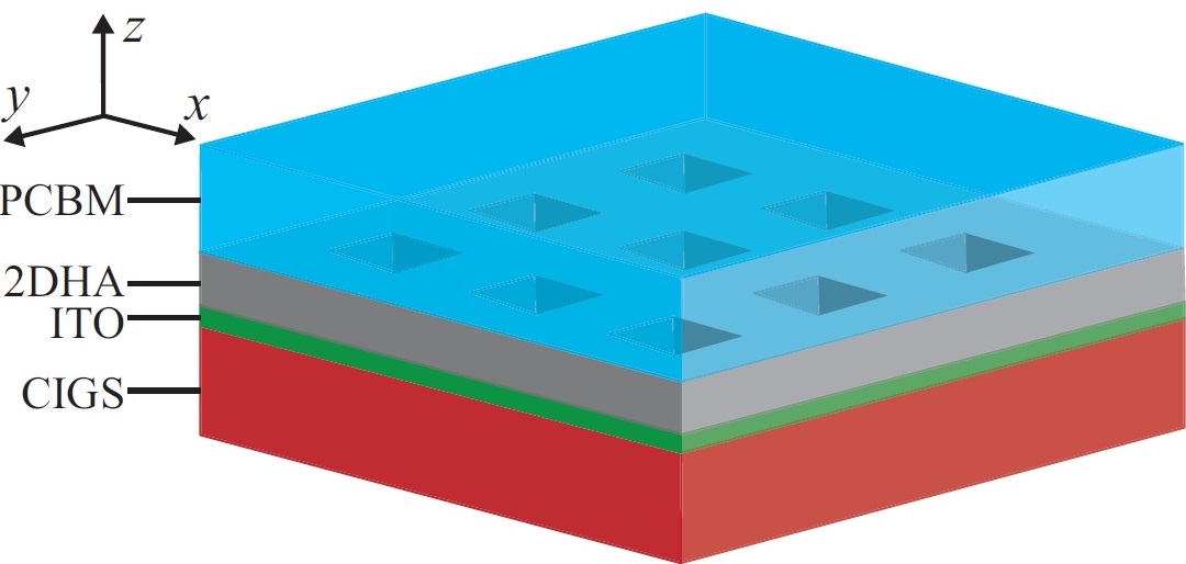
Although ultra-thin-film solar cells can be attractive in reducing the cost, they suffer from low absorption as the thickness of the active layer is usually much smaller than the wavelength of incident light. Different nano-photonic techniques, including plasmonic structures, are being explored to increase the light absorption in ultra-thin-film solar cells. More than one layer of active materials with different energy bandgaps can be used in tandem to increase the light absorption as well. However, due to different amount of light absorption in different active layers, photo-generated currents in different active layers will not be the same. The current mismatch between the tandem layers makes them ineffective in increasing the efficiency. In this work, we investigate the light absorption properties of tandem solar cells with two ultra-thin active layers working as two subcells and a metal layer with periodically perforated holes in-between the two subcells. While the metal layer helps to overcome the current mismatch, the periodic holes increase the absorption of incident light by helping extraordinary optical transmission of the incident light from the top to the bottom subcell, and by coupling the incident light to plasmonic and photonic modes within ultra-thin active layers. We extensively study the effects of the geometry of holes in the intermediate metal layer on the light absorption properties of tandem solar cells with ultra-thin active layers. We also study how different metals in the intermediate layer affect the light absorption; how the geometry of holes in the intermediate layer affects the absorption when the active layer materials are changed; and how the intermediate metal layer affects the collection of photo-generated electron-hole pairs at the terminals. We find that in a solar cell with 6,6-phenyl C61-butyric acid methyl ester top subcell and copper indium gallium selenide bottom subcell, if the periodic holes in the metal layer are square or polygon, total absorption remains approximately the same. However, the total absorption suffers significantly if the holes are triangle. The transmission spectra of incident light into the bottom subcell, and hence the absorption, change significantly for square and circle holes if the active materials change to cadmium selenide (CdSe) and cadmium telluride (CdTe) in the top and bottom subcells, respectively. Although the intermediate metal layer may induce electron-hole pair recombination due to surface defects, the short-circuit current density of an ultra-thin plasmonic solar cell with an intermediate metal layer with two-dimensional hole array is >9% of that of a structure without the intermediate metal layer.
|
|
Publication:
K. Mashooq and M. A. Talukder, "Management of light absorption in extraordinary optical transmission based ultra-thin-film tandem solar cells," J. Appl. Phys. 119, 193101 (2016). [ PDF ]
M A Awal, Z. Ahmed, and M. A. Talukder, "An efficient plasmonic photovoltaic structure using silicon strip-loaded geometry," J. Appl. Phys. 117, 063109 (2015). [ PDF ]
|
| |
|
|
|